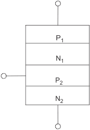
Power Electronics In a P1N1P2N2 thyristor which layer is less doped ? P2. N1. N2. P1. P2. N1. N2. P1. ANSWER DOWNLOAD EXAMIANS APP
Power Electronics Under normal operating condition voltage clamping device offers impedance of high value. low value. moderate value. zero value. high value. low value. moderate value. zero value. ANSWER DOWNLOAD EXAMIANS APP
Power Electronics Rise time is defined by the interval when anode voltage drops from 90 % to 10 % of its initial value. anode current rises 10 % to 90 % of its final value. gate current rises from 90 % to 100 % of it final value. both B and C. anode voltage drops from 90 % to 10 % of its initial value. anode current rises 10 % to 90 % of its final value. gate current rises from 90 % to 100 % of it final value. both B and C. ANSWER DOWNLOAD EXAMIANS APP
Power Electronics The turn-on time of an SCR with inductive load is 20 µs. The puls train frequency is 2.5 KHz with a mark/space ratio of 1/10, then SCR will Turn on if inductance is removed. Turn on. Turn on if pulse frequency us increased to two times. Not turn on. Turn on if inductance is removed. Turn on. Turn on if pulse frequency us increased to two times. Not turn on. ANSWER DOWNLOAD EXAMIANS APP
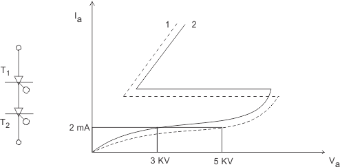
Power Electronics Calculate the maximum voltage that can be safely blocked by the string shown in figure, if maximum allowable leakage current is 2 mA? 10 KV. 8 KV. 6 KV. 2 KV. 10 KV. 8 KV. 6 KV. 2 KV. ANSWER DOWNLOAD EXAMIANS APP
Power Electronics A power MOSFET has three terminals called Drain, source and gate. Collector, emitter and base. Drain, source and base. Collector, emitter and gate. Drain, source and gate. Collector, emitter and base. Drain, source and base. Collector, emitter and gate. ANSWER DOWNLOAD EXAMIANS APP